Via transitions on RF and High speed digital PCBs
- Mar 31, 2023
- 3 min read
Updated: Mar 31, 2023
When dealing with RF and very high-speed digital designs, a lot of engineers tend to focus on impedance control of the traces while forgetting about the layer transitions using vias.
Even on HDI PCBs with impedance-controlled stack-ups that use microvias that are of limited depth (of typically 100um – 150um) and no any stubs, the via transition could degrade return loss if not designed properly.
The reason for this is that PCB manufacturers can only adjust / control trace impedance and not via impedance. Vias, just like traces have inductance and capacitance associated with them and depending on their dimensions could result in significantly different impedance when compared to the traces they connect to.
Via Structure
Vias are simple structures that travel from one copper layer to another helping the traces to carry current from one point to another. They are generally drilled and plated with copper. Most vias are not filled with anything, though in sensitive designs the vias tend to be filled tolerating an additional cost.
The via structure looks as shown in Figure 1 when looked through a PCB. All unfilled vias have a drill hole and plating. A drill hole is generally the finished size of the via hole after it is plated. The vias also have a parameter called clearance or antipads.
The antipads are nothing but spacing between the via plating and the connection to the adjacent copper structure. In Figure 2, via clearance is the gap between the via plating and the surrounding ground layer. By changing the antipad dimensions we can change the capacitance associated with a via and hence directly control its impedance.

Figure 1: Via Structure

Figure 2: Clearance Pads
Theoretical Calculation
When designing a RF PCB, engineers typically simulate the transitions on a 3D EM simulation software like CST or HFSS to understand what via dimensions work with the given trace impedance.
But for simple structures that generally have a return path running underneath the trace, we do not always need to simulate them. Instead, some theoretical analysis can be done to identify, if maximum energy can be transferred or not.
As mentioned before, by varying antipad dimensions, we can match impedance of the via to the trace impedance. (While via drill size can have dramatic effect on impedance, lets maintain the via drill size as constant and change antipad dimensions, since this does not have any consequence on cost.)
Inductance of a via: Lv = 2Lμ0 * ln(b/a)
Capacitance of a via: Cv = 2πε0 / ln(b/a)
where,
L = Length of the via b = Clearance diameter a = Via diameter
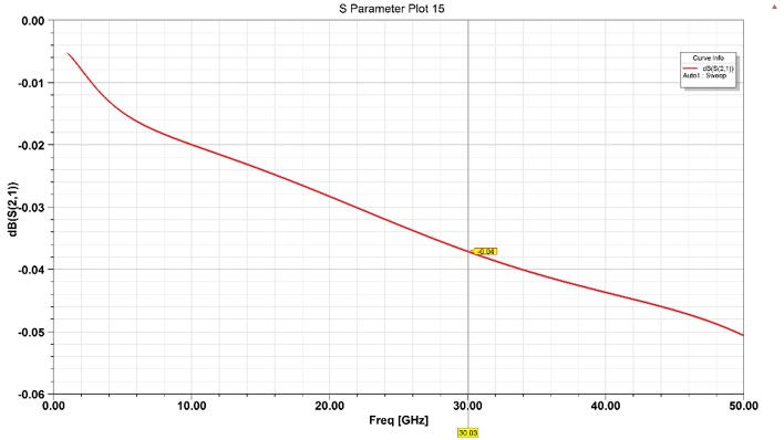
Based on these above equations, we could derive the following table that would provide varying via impedance for varying antipad dimensions. The Theoretical values predict that an antipad radius of 0.6mm or 0.65mm (diameter of 1.2mm and 1.3mm) would provide the best possible return loss for the trace configuration that was considered.

Table 1: Theoretical calculation of impedance
Conclusion
It is a good idea to consider varying antipad dimensions for vias that are located on critical traces when the frequencies of interest are higher.
Theoretically, for a simple design that has the return path underneath the trace, the via impedance can be calculated on a log book.
But for more complex PCBs, it is best to import the design into a 3D solver and work with all the possible return paths for the trace in order to achieve the most realistic results.